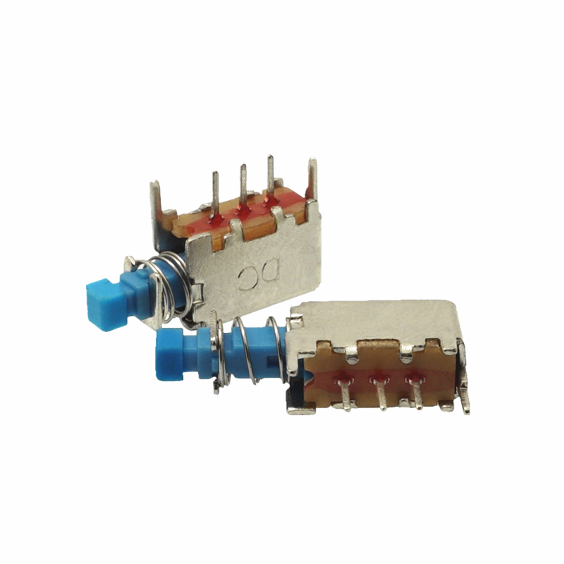
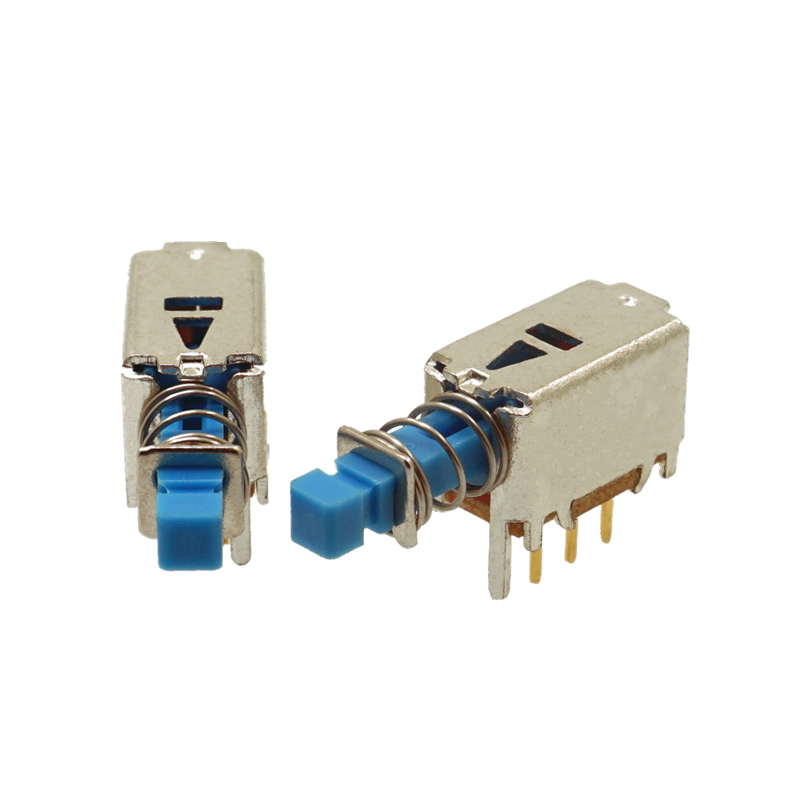
The circuit in this example can be switched on and off through switch S1. Press the first time to turn on, the second time to turn off.
Working process of the whole circuit:
Let's first look at the initial state of the circuit:
When the circuit is powered on, switch S1 has not been pressed. Q1 is off, and Vout has no output. The voltage on capacitor C2 is low. The transistor Q2 is also turned off.
When the switch S1 is pressed, since the voltage on the capacitor C2 is at a low level, when S1 is pressed, the gate G potential of Q1 is pulled down, so that the PMOS transistor Q1 is turned on, and Vout has a power output.
At the same time, the voltage on Vout makes the transistor Q2 saturate and conduct through the voltage dividing resistors R2 and R5, and further pulls down the gate of Q1, so that Q1 can be fully conducted. The circuit is turned on. Capacitor C2 is charged through resistor R1 in preparation for pressing the button again to shut down.
When it is necessary to shut down, press the switch S1, and the high level on the capacitor C2 will also pull up the high level of the gate of Q1, so that the PMOS tube is turned off, Vout has no output, and the base of the Q2 transistor has no bias voltage, and it will also be turned off. The capacitor C2 is discharged through the resistor R1, the load of Vout, and returns to the initial state, preparing for the circuit to start up.
Here the capacitor C3 has a certain anti-interference effect on the load fluctuation.
Note:
The circuit of this example has a defect, so it cannot be used in an actual product. When we turn on the phone, if we hold down S1 for too long, Q1 will be turned off immediately and the machine will be shut down, resulting in a "tail-collision".